PCB design
Designed for your device
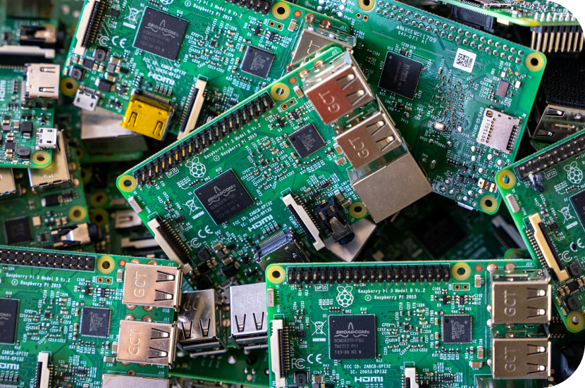
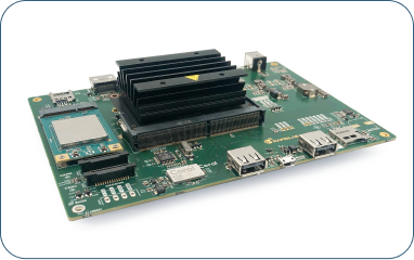
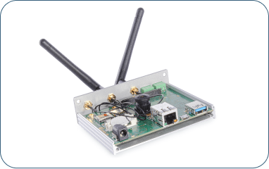
Bespoke electronics bring savings from day one of usage. Let us design and produce your own, custom PCB.
How to order a PCB project?
Send us a request
Send us a request with the general scope of work/project. List the functionalities you care most about and specify in what timeframe the project should be implemented.
We will contact you
We will contact you within 48h of receiving your message to discuss the details. We will propose a solution to your project, select equipment and determine the scope of work together
Receive a quote
You will receive a quotation for your project including detailed specification of proposed hardware, embedded system, documentation and electromagnetic compatibility testing (EMC).
RapidLab is Raspberry Pi Approved Design Partner
Our services
Do you want to enter the market with a product adapted to your requirements? Our engineers have years of experience in creating PCBs from scratch. We base each project on the individual needs of our customers.

Project management
We provide an experienced manager with a history of leading various electronics design projects.
PCB design
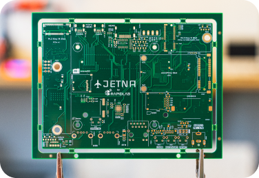
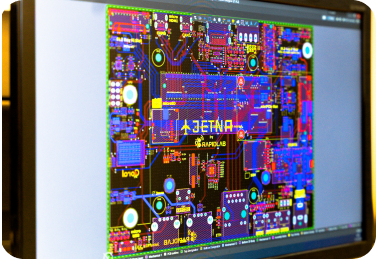
We design a graphic version of the PCB in Altium Designer with all the necessary components.
Implementation
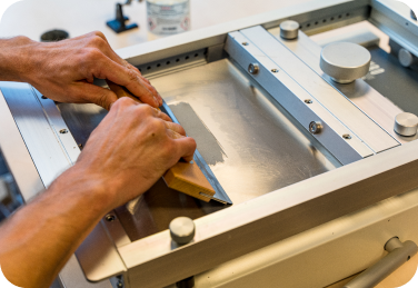
Our engineers personally place the components on PCB on PCB, solder and burn them.
Software
We design software dedicated to a specific PCB, taking into account all the functionalities your project requires.
Tests
EMC and RED testing, including the selection of appropriate standards. We also check the performance of the defined design functionalities.
Documentation
We create complete documentation for each project, including manuals, schematics, layout, and a 3D PCB model.
Ready in 9 weeks or less!
PCB design process
At this stage, the board’s shape, the components’ locations, and the paths between them (so-called routing) are determined. Logos and descriptions for easy assembly and use are also applied.
PCB designing
The 3D view with components is checked. The layout of all the components, as well as the PCB size matching with the case. All parameters have to fit together.
Design review
The last stage of the design involves applying solder paste to specific places on the PCB. All components are also laid out. The board prepared in this way is put into the oven. After removal, the finished product can be tested.
Implementation
See our PCB products
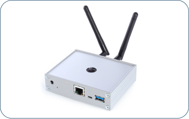
Edge AI face recognition
Identifying people to improve safety or monitor employee attendance.
Empower your project
Unlock the full potential of your technical aspirations!
Contact our experts to explore the possibilities and drive your projects to a new level.
Empower your project
Discover the full potential of technology with experienced engineers.
